High throughput TEM and STEM microscope for all materials science applications.
For scientists to advance their understanding of complex samples and develop innovative materials, they must have access to robust, precise instrumentation capable of correlating form and function, as well as resolving space, time and frequency.
Thermo Fisher Scientific introduces the Thermo Scientific Spectra 200 (S)TEM, the high-throughput, aberration-corrected, (scanning) transmission electron microscope for all materials science applications.
Built on an ultra-stable foundation
All Spectra 200 (S)TEM's are delivered on new platforms designed to offer an unprecedented level of mechanical stability and highest imaging quality though passive and (optional) active vibration isolation.
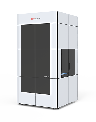
The system is housed in a fully re-designed enclosure with a built-in on-screen display for convenient specimen loading and removal. For the first time, full modularity and upgradeability can be offered between uncorrected and single-corrected configurations with variable heights, allowing maximum flexibility for different room configurations.
The Spectra 200 (S)TEM can be powered by a new-cold field emission gun (X-CFEG). The X-CFEG has extremely high brightness (>>1.0 x 10⁸ A/m2/Sr/V*), low energy spread, and can be operated from 30 – 200 kV. This provides high-resolution STEM imaging with high probe currents for high-throughput, fast acquisition STEM analytics. With the powerful combination of X-CFEG and S-CORR probe aberration corrector, sub-Angstrom STEM imaging with over 1000 pA of probe current can be routinely achieved.
Si[110] HAADF images taken on a Spectra 200 S/TEM with probe currents ranging from 0.016 nA up to 1 nA while maintaining <76 pm STEM resolution.
Further, probe currents can be flexibly tuned from <1 pA up to the nA range with fine control of the gun and condenser optics, all with minimum impact on the probe aberrations, so that the widest range of specimens and experiments can be accommodated (see the MOF example in the Panther STEM detection section).
As with all cold field emission sources, the sharp tip requires a periodic regeneration (called flashing) to maintain the probe current. With the X-CFEG, the tip only requires flashing once per working day, a process that takes less than a minute. There is no measurable impact on the probe aberrations even in the highest resolution imaging conditions and the daily tip flashing process has no impact on the tip lifetime.
Tip flashing on the X-CFEG: 60 pm resolution at 200 kV is maintained before and after a tip flashing without adjustment of the optics. The process takes less than one minute and is required only once per working day and has no impact on the lifetime of the tip.
This new generation X-CFEG also produces enough total beam current (>14 nA) to support standard TEM imaging experiments (e.g. in situ) with large parallel probes, making it a uniquely all-purpose, yet high-performance, C-FEG.
The combination of enhanced mechanical stability, the latest 5th order S-CORR probe aberration correction and the X-CFEG, gives the Spectra 200 (S)TEM high-resolution, high-contrast STEM imaging capability for all accelerating voltages. Additionally, Spectra 200 (S)TEM retains the wide gap S-TWIN objective lens as standard from the Themis product line, to ensure customers have a pole gap with “room to do more” without compromising on spatial resolution. In the images below, 48 pm resolution is shown on a wide gap S-TWIN Spectra 200 (S)TEM at 200 kV.
Adding to ease of use, the Spectra 200 (S)TEM includes smart software algorithms to quickly, reproducibly and reliably correct up to 4th order aberrations in the STEM probe (Auto S-CORR) and optimize 1st and 2nd order aberrations on any specimen (OptiSTEM+). Auto S-CORR can therefore be used on a weekly basis to maintain high-order aberrations and OptiSTEM+ can be used daily to optimize image quality without the need of a standard specimen or manual tuning.
Si [110] and GaN [212] taken on a Spectra 200 (S)TEM showing the specified resolution on a wide gap analytical S-TWIN pole piece (green circle) and achievable resolution (red circles). At 60 kV, 96 pm resolution is specified and at 200 kV, 60 pm is specified with an achievable resolution <48 pm.
STEM imaging on the Spectra 200 (S)TEM has been re-imagined with the Panther STEM detection system, which includes a new data acquisition architecture and two new, solid state, eight-segment ring and disk STEM detectors (16 segments in total). The new detector geometry offers access to advanced STEM imaging capability combined with the sensitivity to measure single electrons.
The 16 segmented ring and disk detectors of the Panther STEM detection system allow for a range of STEM signals without the need for multiple detectors.
The entire signal is optimized and tuned to provide unprecedented signal-to-noise imaging capability with extremely low doses to facilitate imaging of beam sensitive materials. Additionally, the completely redeveloped data acquisition infrastructure can combine different individual detector segments, with the future possibility of combining detector segments in arbitrary ways, generating new STEM imaging methods and revealing information that is not present in conventional STEM techniques. The architecture is also scalable and provides an interface to synchronize multiple STEM and spectroscopic signals.
Comparison SrTiO₃ [001] HAADF images taken with the Panther STEM detection system with 3 pA, 1.3 pA and <1 pA of probe current. Even with probe currents <1 pA, the signal-to-noise ratio in the image allows automation routines like OptiSTEM+ to correct 1st and 2nd order aberrations in the probe forming optics, delivering sharp images.
Metal Organic Framework (MOF) MIL-101 imaged with 0.5 pA of beam current in STEM with iDPC at 200kV. The image is a single shot with a frame time of 23.5 seconds and the complex structure can be seen with 2 Å resolution. (Specimen courtesy of Professor Y. Han, King Abdullah University of Science and Technology.)
The Spectra 200 (S)TEM can be configured with an electron microscope pixel array detector (EMPAD) or a Thermo Scientific Ceta Camera with speed enhancement to collect 4D STEM data sets.
The EMPAD is capable of 30-300 kV and provides a high dynamic range (1:1,000,000 e- between pixels), high signal-to-noise ratio (1/140 e-), and high speed (1100 frames per second) on a 128 x 128 pixel array, which makes it the optimal detector for 4D STEM applications. (E.g. Applications where the details of the central and diffracted beams need to be analyzed simultaneously, as in the ptychography image below.)
The EMPAD detector can be used for a wide variety of applications. On the left, it is used to extend spatial resolution (0.39 Å) beyond the aperture limited resolution at low accelerating voltages (80 kV) in a bi-layer of the 2D material MoS2 (Jiang, Y. et al. Nature 559, 343–349, 2018) . On the right, it is used to independently image dark field reflections, revealing the complex microstructure of the precipitates in a superalloy (Sample courtesy Professor G. Bourke, University of Manchester).
The Ceta Camera with speed enhancement offers an alternative for 4D STEM applications where a greater number of pixels is required and when EDX analysis needs to be combined with each point in the STEM scan. This solution provides higher resolution diffraction patterns (up to 512 x 512 pixel resolution), suited for applications such as strain measurement.
The Spectra 200 (S)TEM has been configured to be a STEM analytics powerhouse. The extreme brightness and low energy spread of the X-CFEG, the latest generation, 5th order S-CORR probe corrector, the wide gap (S-TWIN or X-TWIN) pole piece with a portfolio of large solid angle and symmetric EDS detectors and the built-in EDX quantification engine in Thermo Scientific Velox Software makes STEM EDX on Spectra 200 (S)TEM fast, easy and quantifiable.
The Thermo Scientific EDX detector portfolio provides a choice of detector geometries to suit your experimental requirements and optimize EDX results. Both configurations have a symmetric design (see below), producing quantifiable data. Note that holder shadowing as a function of tilt is compensated in both detector configurations via built-in Velox Software functionality.
The Spectra 200 (S)TEM can be configured with either Super-X (for spectrum cleanliness and quantification) or Dual-X (for the largest solid angle and high-throughput STEM EDX mapping).
The Super-X detector system provides a highly collimated solid angle of 0.7 Sr and a Fiori number greater than 4000. It is designed for STEM EDX experiments where spectral cleanliness and quantification are critical.
The Dual-X detector system provides a solid angle of 1.76 Sr and a Fiori number greater than 2000. It is designed for high-throughput STEM EDX experiments such as EDS tomography or where signal yield is low and fast mapping is critical.
In the example below, the DyScO3 perovskite system is examined with the Dual-X detectors. The ultra-high brightness (>>1.0 x 10⁸ A/m2/Sr/V*) of the X-CFEG and the resolving power of the S-CORR probe corrector are used to deliver a probe to the specimen with 150 pA of current and size <80 pm. With these high-brightness probe conditions, EDX mapping can be done rapidly with high sampling and high SNR, resulting in, for the first time, sub-Å spatial information in a single elemental, raw, and unfiltered EDX map. A fast Fourier transform of the Sc map shows up to 90 pm resolution.
DyScO3 specimen investigated with the powerful combination of ultra-high brightness X-CFEG, S-CORR and the large solid angle (1.76 Sr) of the Dual-X detectors, resulting in high signal-to-noise ratio, atomic resolution (up to 90 pm), unfiltered EDX maps (Sample courtesy Professor L.F. Kourkoutis, Cornell University).
Electron energy loss spectroscopy on Spectra 200 (S)TEM has also been accelerated by the ultra-high brightness (>>1.0 x 10⁸ A/m2/Sr/V*) and intrinsically high energy resolution (<0.4 eV) of the X-CFEG which are delivered simultaneously in the STEM probe.
In the figure below, a probe with narrow energy spread (0.36 eV) and high current (480 pA) high spatial resolution (65 pm) provides ideal conditions to collect the Dy, Sc and O core loss edges with high energy resolution, signal to noise ratio and spatial resolution in the STEM image.
DyScO3 specimen investigated with a Spectra 200 (S)TEM. The combined ultra-high brightness of the X-CFEG, intrinsically low energy spread of the source (<0.40 eV) and resolving power of the S-CORR results in high signal-to-noise ratio, Sc, O and Dy core loss edges with a sub-70 pm STEM probe (Sample courtesy Professor L.F. Kourkoutis, Cornell University).
 images of silicon.")
 images of GaN and silicon.")

 images of SrTiO3.")

 image of MoS2.")

